
AMD Zen 5 architecture: A ground up redesign that lays the foundation for future Ryzen CPU architectures
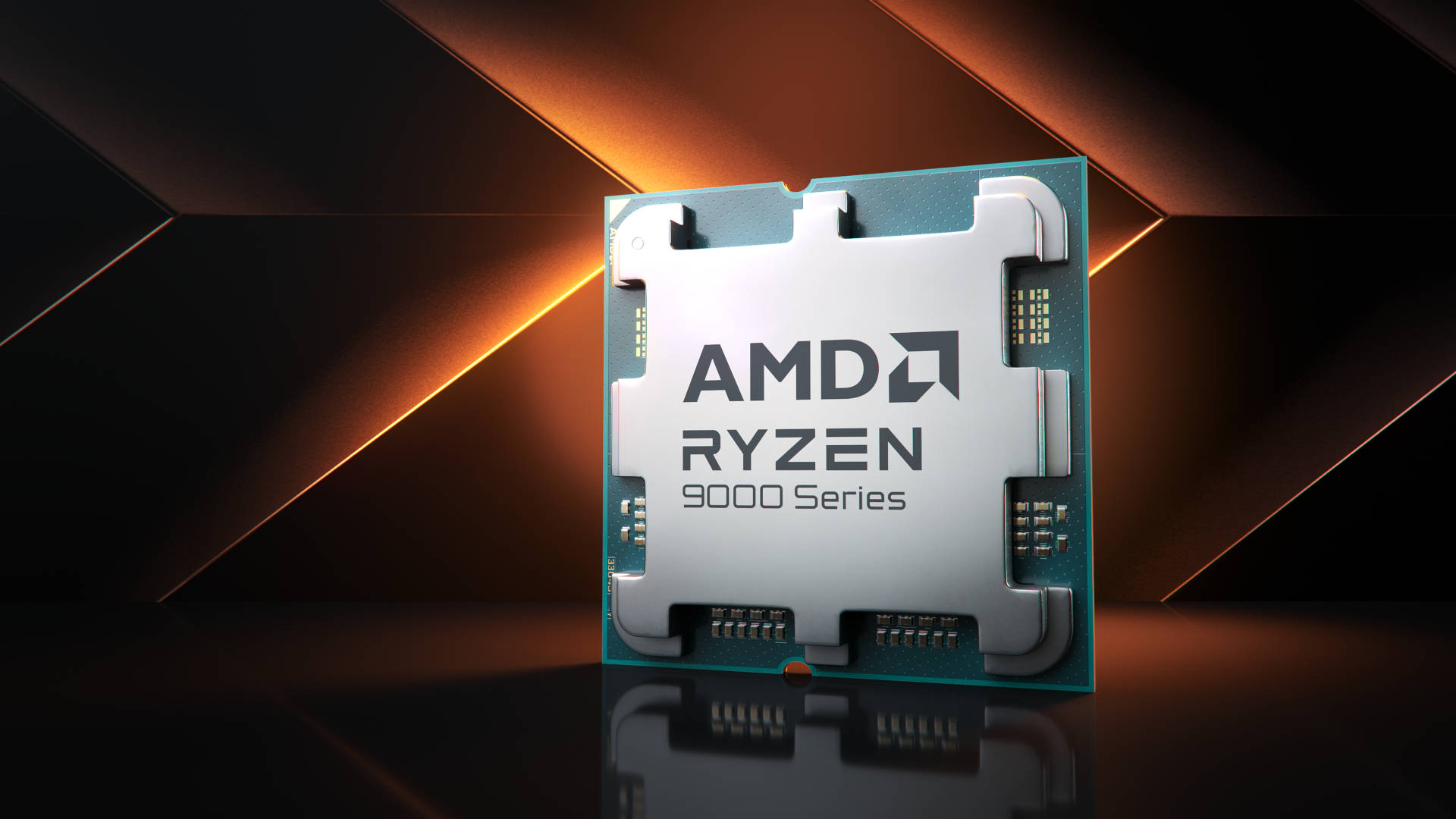
AMD is confident a 16% IPC uplift will see its Ryzen 9000-series ascend the CPU silicon throne.
The AMD Zen 5 CPU architecture will form the backbone of the next generation of Ryzen desktop and laptop processors, and while we got a general idea of the new tech during the Computex unveiling a month back, we've now been treated to the full architecture monty. I've spent the past week immersed in the new Ryzen technology at the recent AMD preview event in LA and, although we'll have to wait a little longer to see just how much oomph the new chips have, we now have much more information about what makes Zen 5 tick.
With improved cache, with more bandwidth and an expanded execution window, we feed the beast.
Mark Papermaster, AMD
Before diving into the finer details, it's worth revisiting the information revealed back at the start of June. At Computex 2024, AMD announced the Zen 5-based Ryzen 9000-series desktop CPUs and Ryzen AI 300 mobile APUs were set to launch during the month of July. As was expected, Dr Lisa Su's Computex keynote was full of general details for a general audience, with little meat on the bone regarding the architecture itself.
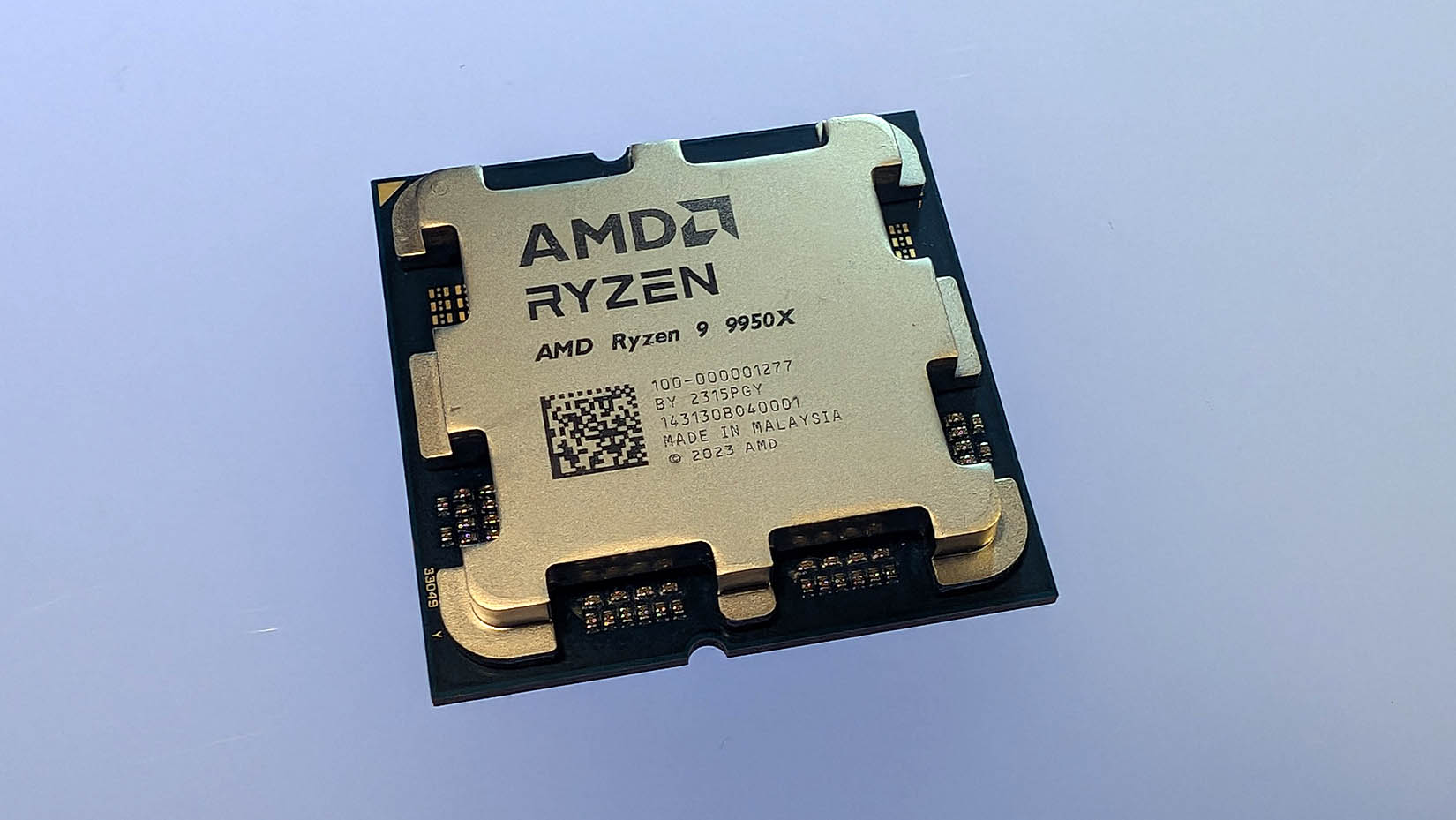
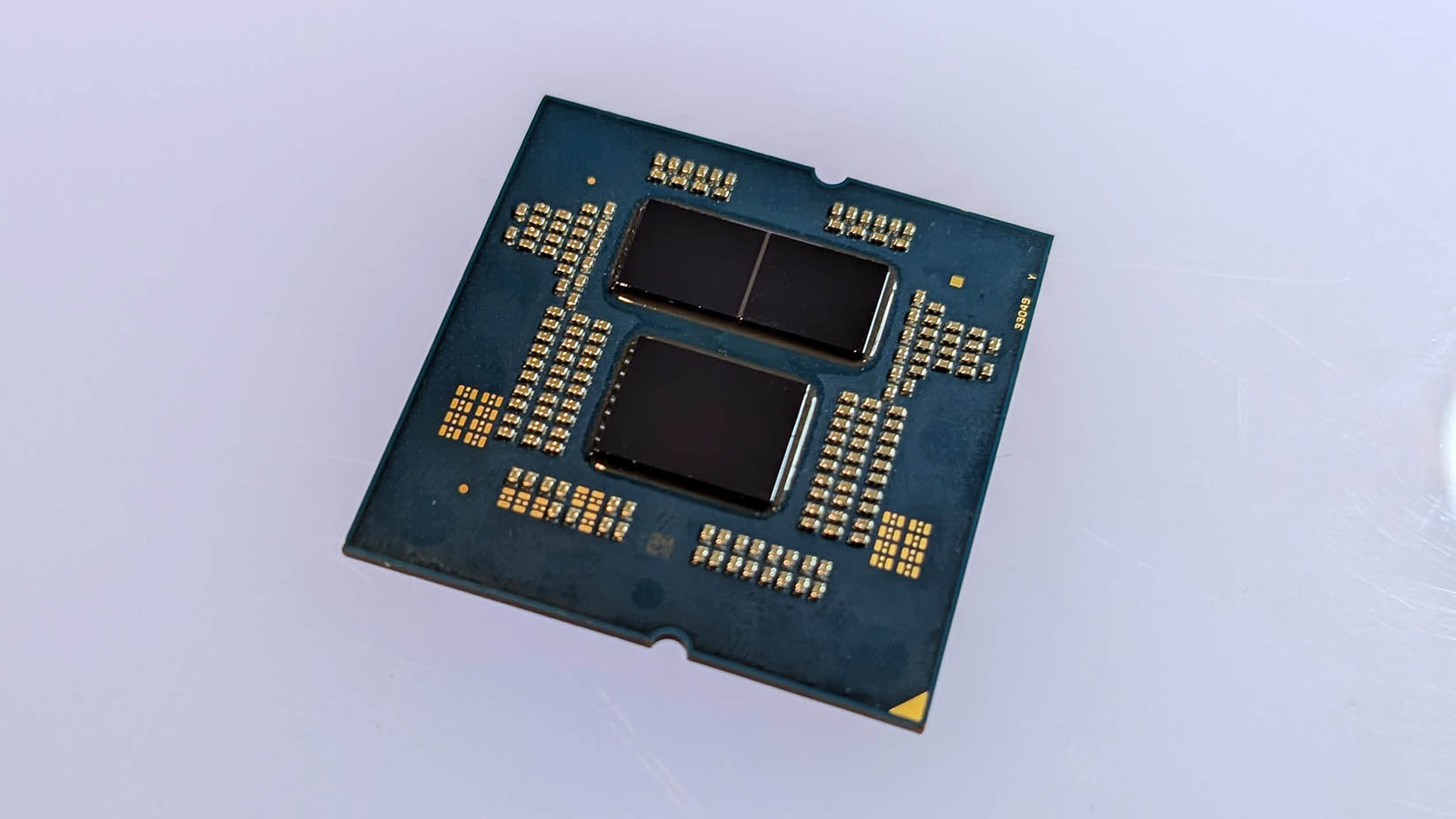
The Ryzen 9000-series is codenamed Granite Ridge. And, apart from the architectural improvements, the new models are physically similar to their Ryzen 7000-series predecessors.
The CCDs, or Core Complex Dies are still made up of eight cores, with a shared 32MB of L3 cache. The Ryzen 9 9950X and 9900X come with two CCDs, while the Ryzen 7 9700X and Ryzen 5 9600X only need one. All chips include a separate I/O die, which is the same as that used with Zen 4.
Granite Ridge includes an RDNA2 integrated GPU with two compute units. The CCDs are manufactured with TSMC's N4 process, while the I/O die is fabbed on TSMCs N6 process.
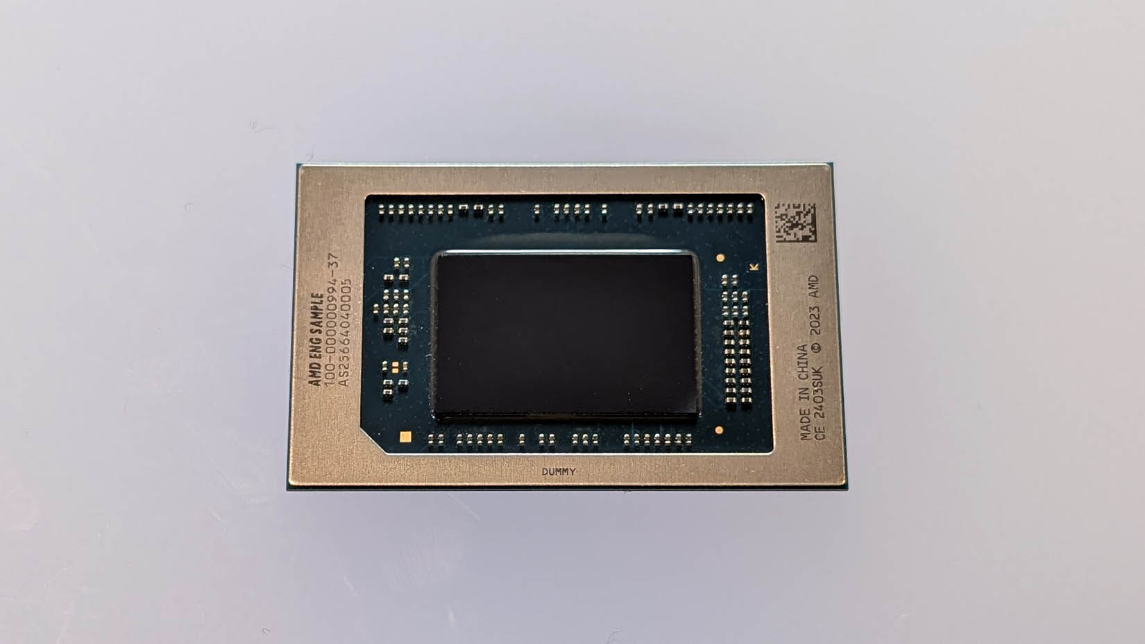
Strix Point mobile APUs come with monolithic dies, and its a large one at that. They're being branded as the Ryzen AI 300 series. You just know that AI had to be placed in that name didn't you? Two models have been announced so far. They are the Ryzen AI 9 HX 370 and Ryzen AI 9 365. These feature 12 cores / 24 threads and 10 cores / 20 threads respectively. Both chips' CPU cores are based on the Zen 5 architecture. Both include an XDNA 2 NPU capable of up to 50 TOPS, and RDNA 3.5 integrated graphics.
The Ryzen AI 9 HX 370 features Radeon 890M graphics with 16 CUs, while the Ryzen AI 9 365 features Radeon 880M graphics with 12 CUs. AMD demonstrated laptops with 890M graphics running the very demanding Cyberpunk 2077 at 1080p at above 55 FPS, albeit with FSR and AFMF activated.
As they are Ryzen 9 models, these chips will find their way into high performance notebooks. Ryzen 7 and Ryzen 5 models are sure to follow later in the year.
Strix Point features a mix of higher performing Zen 5 cores and efficiency focused Zen 5c cores. These aren't like Intel's hybrid P and E-cores though, Zen 5c cores are the same as the larger cores, though they come with less L3 cache and lower clocks. This saved die space, allowing AMD to allocate its transistor budget to other areas, such as the NPU and GPU. AMD says this approach doesn't require software awareness or anything like an on-chip Thread Director that Intel designs do. The 5c cores simply kick in lower on the voltage / frequency curve, when the larger cores would be power limited anyway.
AMD Zen 5 architecture
AMD attributes most of the Zen 5 improvements to four key areas. They are instruction fetch and decode, integer execution, load and store, and the floating point/math execution units.
The front end redesign includes improved branch prediction with lower latency, better accuracy and greater throughput. Branch prediction is one of the fundamental pillars of x86 performance. The better it is, the fewer clock cycles get wasted, leading to better performance and power efficiency. The aim is "to keep the beast fed" as AMD colourfully put it. Downstream, Zen 5 includes dual port instruction and op caches, so it includes not just better branch prediction, but more predictions per cycle. Zen 5 also includes dual decode pipes, whereas Zen 4 included only one.
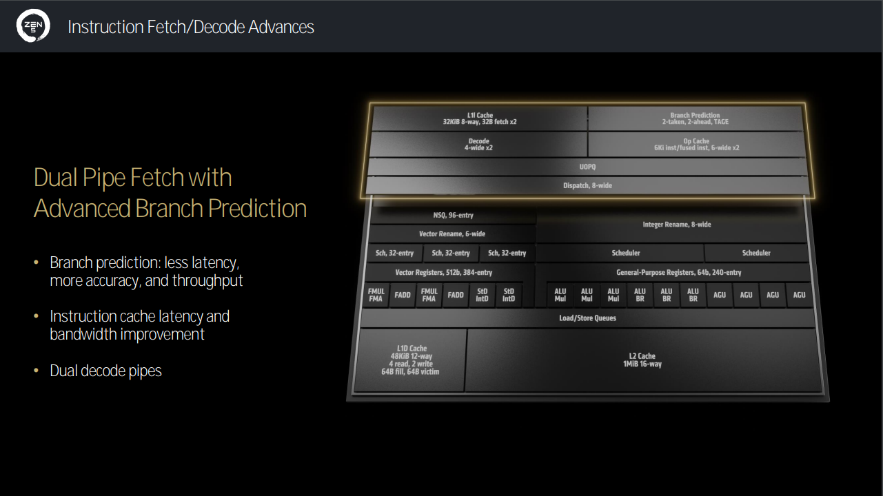
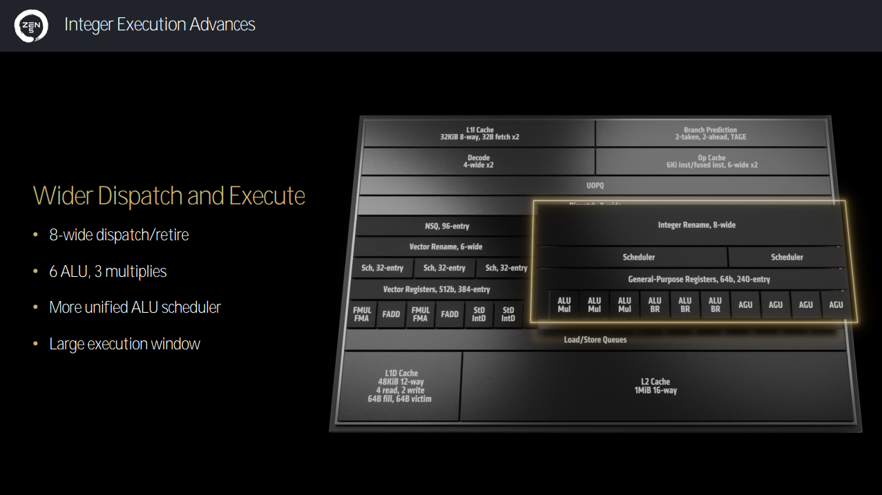
As improved predictions and instructions are coming through the wider pipeline, AMD needed to make improvements to its instruction dispatch and execution engine. This engine now includes eight-wide instruction dispatch and retire capability each cycle, an increase from the six of Zen 4. With more instructions comes the need for improved scheduling, and to this end AMD redesigned its ALU scheduler, which is now more unified than that of Zen 4. Zen 5's retire queue/reorder buffer is 40% larger than the 320 ops of Zen 4 at 448 instructions deep, giving the CPU a wider window of instructions for out-of-order execution. The Arithmetic Logic Unit (ALU) count has been increased to six from Zen 4's four.
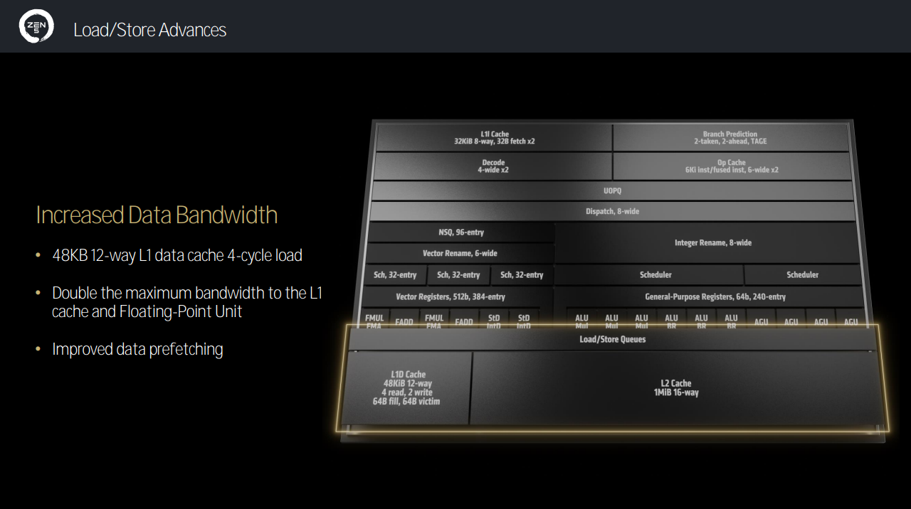
We all love more bandwidth, and the load and store functions of CPUs are no different. The 12-way L1 data cache is now 48Kb in size, up from the 8-way 32Kb of Zen 4. That's a whopping 50% increase, and AMD engineers did it without any latency increase, which is usually the case with larger caches. This L1D cache supports four loads per cycle. AMD says this is particularly beneficial for 512-bit loads. The L1 to L2 bandwidth has also doubled and the prefetching algorithms have been tweaked.
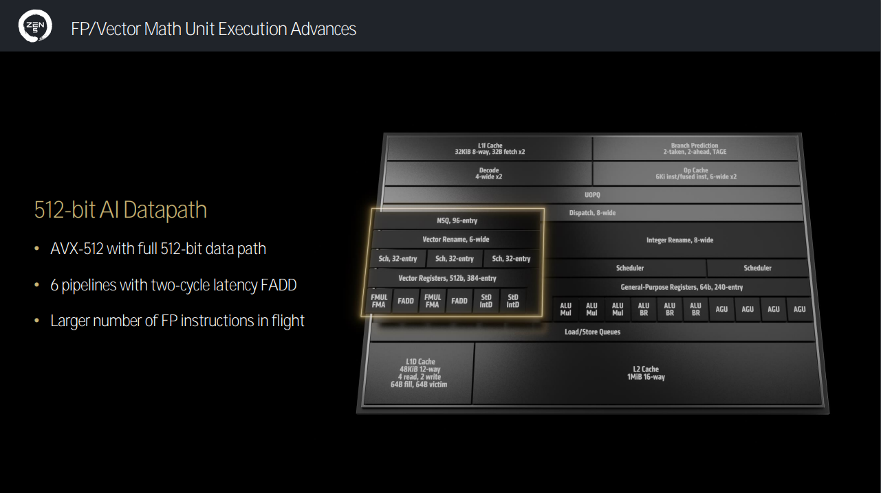
The final key Zen 5 improvements are to the floating point/vector math units. Zen 5 now supports native AVX-512. Zen 4 achieved this by 256-bit double pumping. Interestingly, AMD says Zen 5 processors will run AVX-512 without any frequency penalty. Strix Point supports full AVX-512 too which will remain challenging for notebook cooling and TDPs, though AMD says it still supports the 2x256-bit option depending on the configuration. Note that several of the particularly favorable pre-release AMD benchmarks take advantage of full AVX-512. Machine learning is another field that will benefit from AVX-512 instructions.
AMD Zen 5 performance
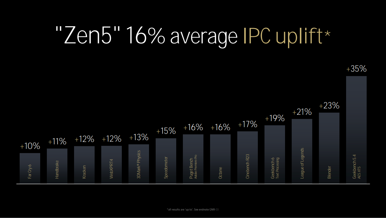
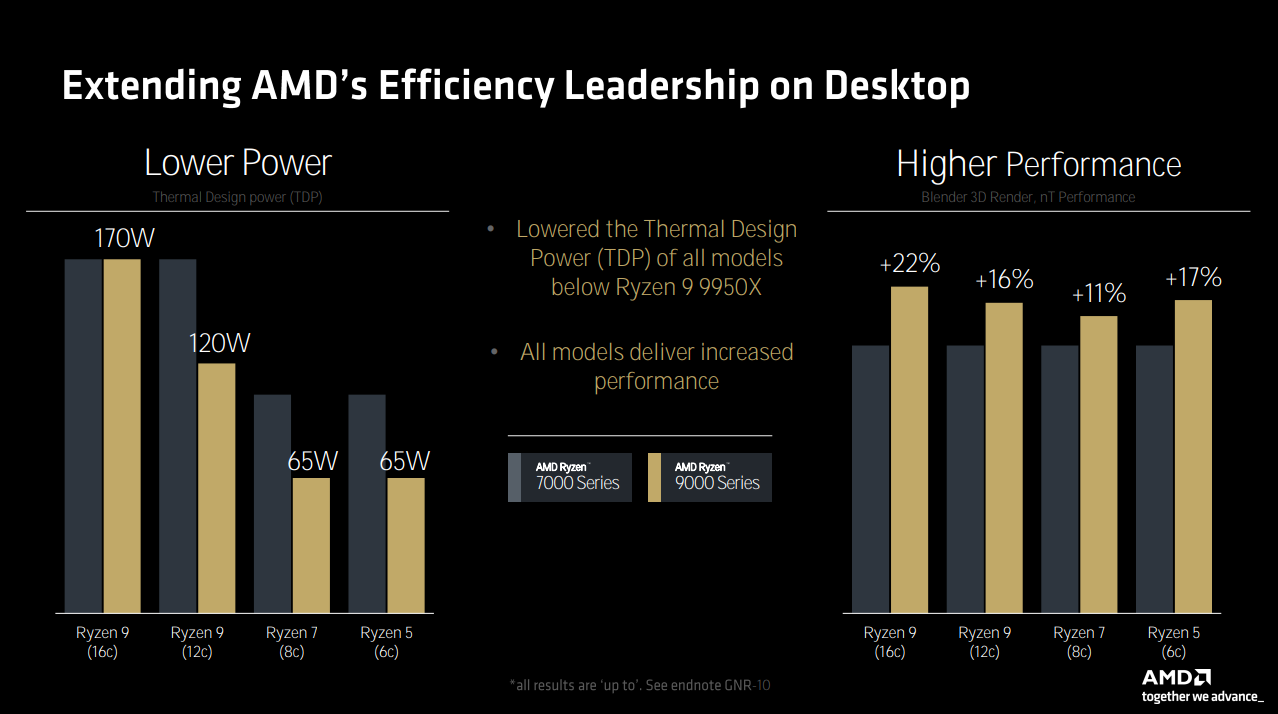
So, the Zen 5's front end has been dramatically improved, as have the execution units. Latency is lower, and throughput and bandwidth have increased, all while keeping power consumption in check. In the case of Granite Ridge, all the SKUs have lower TPDs than their predecessors, with the exception of the Ryzen 9 9950X, which is the same. AMD is understandably quite proud of its 16% average IPC uplift. The gaming improvements are likely to be less overall, but do note the League Of Legends uplift at a seriously impressive 21%.
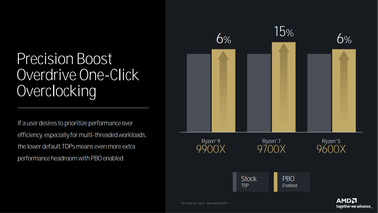
The lower TDPs give users some additional Precision Boost Overdrive headroom, particularly in the case of the 9700X, where AMD claims users can gain as much as 15% higher performance. You'll get even more if you use Curve Optimizer and the new Curve Shaper tool. The latter allows users to tweak the underlying voltage curves to maximize performance.
No NPUs, temps, and RAM overclocking
One of the interesting omissions from Ryzen 9000-series processors is a dedicated NPU. Why, you might ask? I asked AMD Corporate Fellow and Chief Zen Architect Mike Clark about this, and the answer was illuminating. Including an NPU wasn't deemed essential given that most Ryzen 9000 systems will include discrete GPUs, which are already highly capable AI processors. Granite Ridge also includes the AVX512-VNNI (Vector Neural Network Instructions) instruction set. AMD believes a complete redesign of the I/O die was therefore not justified. Time will tell if this design choice was the right one.
Ryzen 9000 series chips reportedly have a 15% thermal resistance improvement, leading to an average 7°C temperature reduction at the same TDP. It's no secret that Ryzen 7000-series chips got a bit toasty, so this will be a welcome improvement and it should allow 9000-series chips to hold higher clocks without thermal throttling with less-than-stellar cooling solutions.
One of the more eyebrow raising features is support for on-the-fly memory overclocking. For example, you could use Ryzen Master to increase your memory speed for gaming, while lowering it for daily use.
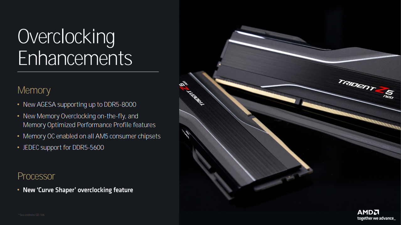
DDR5 support has increased to 5600 MT/s 'officially', with EXPO profiles up to 8000 MT/s also supported. If you recall at Computex, G.Skill demonstrated a Ryzen 5 8500G system running DDR5-10600 memory. AMD says Granite Ridge should be capable of even more. I heard DDR5-11000 mentioned, though that number is likely out of reach without extreme cooling. AMD says the sweet spot for Zen 5 remains in the 6000 to 6400 MT/s range in terms of compatibility, cost, and performance.
But, as DDR5 speeds are continually on the rise it will be interesting to see whether memory in the 8000 MT/s+ range could end up making some sense for gaming, as higher frequencies will eventually deliver enough raw speed to overcome the latency penalty you get when running 1:2 mode on the memory controller. That's something I personally look forward to testing.
AMD Zen 5 motherboards
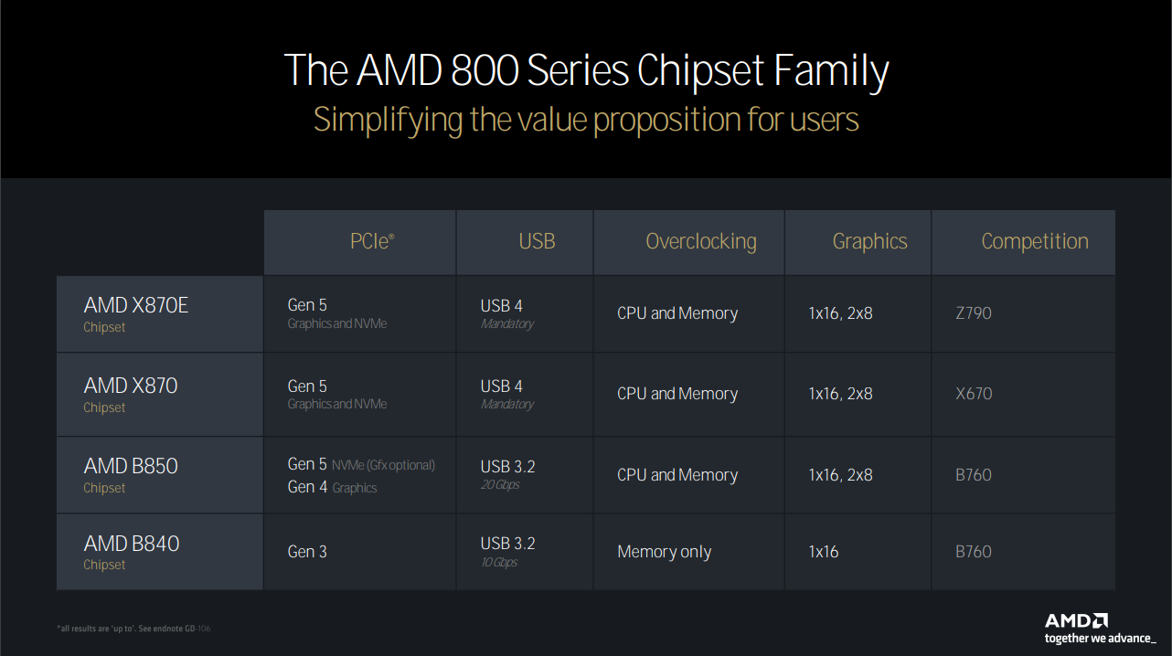
We got a good look at the specifications of the upcoming 800-series chipsets. There's little that's revolutionary here, though mandatory USB 4 is welcome on X870E and X870 motherboards. It is disappointing to see PCIe 3.0 support only for entry level B840 motherboards. That could throw up issues for future graphics cards with x4 or x8 interfaces.
AMD X3D and future Zen
I asked AMD about how the Ryzen 7800X3D compares to the Ryzen 7 9700X in gaming. The answer I got was that the 9700X should squeak ahead on average, though cache-loving games will favor the 7800X3D.
On a related note, AMD pointed out that the 9700X is on average 13% faster than the Ryzen 7 5800X3D. This will give AM4 gamers a little incentive to make the switch, though 9000X3D chips will be worth waiting for if you are on the fence about switching to AM5. Of course, AMD gave an entirely expected 'no comment' when I asked about 9000X3D chips, but you can be sure that such chips are coming. AMD will be hoping to take some wind out of the sails of Intel and its upcoming Arrow Lake processors, which are coming later this year.
It's a pedestal that we'll use to build the next several generations of Zen
Mark Papermaster, AMD
One of the little things I picked up on is that AMD designed Zen 5 to be a foundational architecture. The front end improvements were designed to do what AMD phrased as "keeping the beast fed". Though AMD cannot be expected to comment on future architectures, I do wonder if some of the groundwork is there to enable Zen 6 to scale to higher core counts.
Only AMD will know what bottlenecks can be improved upon, or if there is some low hanging fruit waiting to be picked. The latter is unlikely given the historical difficulty of achieving significant inter-generational x86 IPC improvements along with the slowing down of Moore's Law.
We won't have long to wait and see if AMD's confidence is justified. Ryzen 9000-series CPUs are due to launch on July 31, with Ryzen AI 300-series laptops due imminently, depending on the OEM.